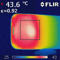
Thermal Imaging

To show so-called hotspots in electronic products we use the method of thermal imaging. A great advantage of thermal imaging is related to the contactless temperature measurement.
This enables us to capture also small components and elements to be detected where measurements by means of contact sensors are impossible.
Thus weak points in circuit design can be identified and safety-relevant problems can be discovered.
We recognize weaknesses
early in the development
phase.